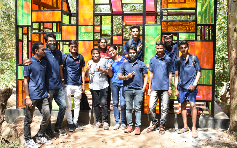
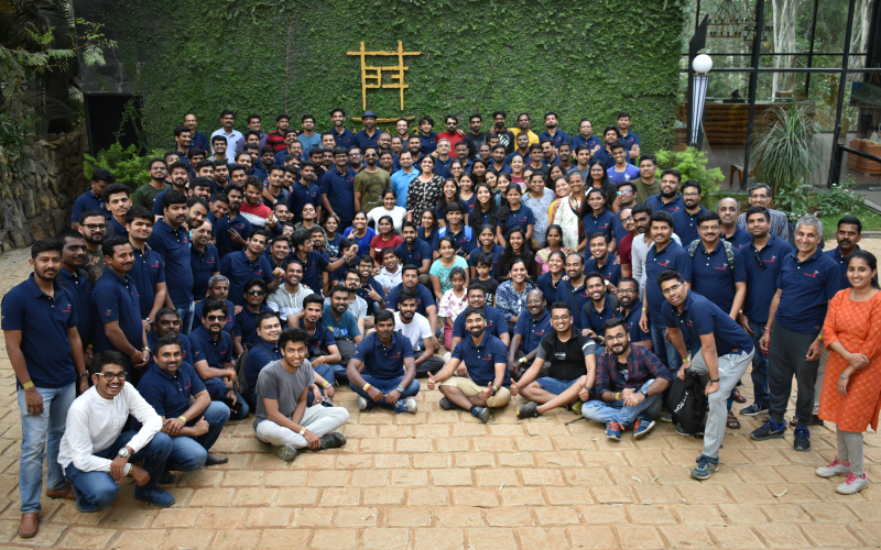
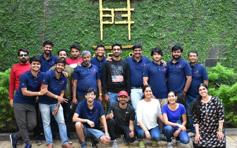
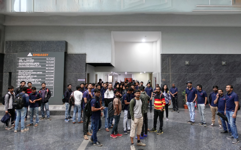
Life@Saankhya
Driving innovation by working at Saankhya Labs
A fertile-ground for ideas that can be developed into innovative products – that’s who we are, at Saankhya Labs. Yet, this alone doesn’t define us entirely. We are also a 200+ strong team comprising some of the most unconventional minds, unique technological expertise, one-of-its-kind experiences, lots of fire in the belly and a shared goal to play an integral role in shaping the future of communication technology, by raising the bar continuously and challenging status quo.
And this is what we look for in people who would like to join us. Attracting and developing like-minded talent has been important area of focus at Saankhya Labs. We are looking for people who have innovation built in their DNA, because we know they’ll feel at home with us. So, before you apply, here’s a quick look at what you can expect, once you get here.
- Though we started in 2006, you’ll find that we still work with the energy and informal mindset of a start-up.
- We work on truly next gen technologies – so cutting edge, that you’ll seldom find it elsewhere in the world.
- Our code of ethics drives us to go beyond compliance and build sustainable solutions to complex business and societal challenges.
- We have an environment that fosters opportunities to work on the most exciting technologies, applications, projects and roles.
- We believe in a relatively flat organizational structure, with less supervision and more self-driven, responsible teams.
- Involvement in building prototypes, the likes of which become industry benchmarks will soon become second nature to you here.
- We work in an inclusive atmosphere and believe that merit is the only criteria for advancement.
- We believe in balancing work and personal life with a range of workplace options and innovative tools that help us stay connected.
Check out our open positions for further details.


Job Openings
Open Positions – Full Time
LOCATION : Bangalore
EXPERIENCE REQUIRED
- 10-25 years’ experience.
JOB DESCRIPTION
- Involve in design and development of a breakthrough “from-the-scratch” compiler and associated toolchain based on a Domain Specific Language (DSL) used in 5G Telecom development. The toolchain and language are conceptually similar to “SyCL/OpenCL” but applied to wireless domain.
- To play major role in language/framework design as well as Intermediate Representation (IR) design.
- Involve in development of corresponding tool-chain i.e. compiler, simulator, code generator, debugger
- To be a part of a larger system programming team and lead the architecture & methodology definition right up to implementation of the toolchain
- To work with other experts to solve some of the most complex problems in the field of development tools that you might encounter in the industry
- To work on making a ding in the universe.
REQUIREMENTS
- Sound knowledge of C, C++ 14 especially template meta programming with great programming skills.
- Sound knowledge of Data Structures and algorithms
- Strong knowledge of Compiler tool development or any EDA/ESL tool development.
- Exposure to heterogeneous compute environments
- Familiarity with GPU/DSP or heterogenous compute, CUDA, openCL etc. or gcc/LLVM/Clang development.
ADDED ADVANTAGE
- Excellent verbal and oral communication in English
- Experience with interacting with customers and multi-disciplinary teams
- Self-learner, highly motivated, self-paced
- System Programming Languages like Rust/Golang
JOB DESCRIPTION
- The candidate will be responsible for design and development of satellite communication physical layer standards
- Interfacing to the SW/DSP/Algorithms teams to translate DSP algorithms to custom SOC/DSP firmware (Fixed point C & VLIW/SIMD
assembly) - System integration & verification of algorithms on DSP (HW/controller interfacing, FW/SW partitioning, module/ system level testing)
- Analyzing and debugging the system issues (field trails, compliance tests, customer support)
- Optimizing system performance w.r.t MIPS/Memory/Latency requirements
EXPERIENCE REQUIRED
- 2-9 years in relevant domain
SKILLS
- Experience in physical layer implementation for satellite wireless technology
- Experience in physical layer SW development (Layer1 Control/DSP)
- Experience in embedded software development
- Programming in C/C+ +, Matlab and VLIW/SIMD assembly on processors like c64x/Blackfin etc.
- Excellent analytical and debugging skills
- Prior experience with chipdevelopment/commercialization is a plus
JOB DESCRIPTION
- Design, Development & verification of Physical Layer Algorithms/Models for Wireless (Physical Layer) communications (standard and non-standard waveforms) in MATLAB and C/C++, towards the Development of cutting- edge Next Generation 5G Hardware and Chipsets.
- Fixed- and Floating-point implementations various components of Physical Layer.
- Setting up Standard flows (including Automation) for the Fixed-point designing of the Physical Layer implementations and ensuring its adherence.
- Design, Development, and maintenance of Physical Layer Fixed Point Libraries.
- Define, implement & debug of unit/subsystem/full system test cases.
- Collaborate with Physical Layer Design, System, Hardware, firmware, and Verification teams during Design, Development, and Debugging.
- Collaborating with the DSP Firmware team in Implementation & optimizations of signal processing, Signal Conditioning, and FEC modules.
- Actively support the analysis & debugging of issues arising out of the various system, field, conformance, and operator verification.
ABOUT THE CANDIDATE
EXPERIENCE
- 2-4 Years’ experience in Wireless Baseband/ PHY Algorithm Development
EDUCATION
- Must be B. E/ B. S/ B. Tech/ M.S/ME/M.Tech/PhD in Electronics and Communication (Related branches will be considered)
- Strong academic background with excellent oral and written communication
SKILLS
- Experience in fixed-point modeling of Physical Layer systems in C/C++/MATLAB.
- Experiences in using scripting tools like Perl, Tcl/Tk, python
JOB DESCRIPTION
- Design, Development & verification of Physical Layer Algorithms/Models for Wireless (Physical Layer) communications in MATLAB and C/C++, towards the Development of cutting-edge Next Generation 5G Hardware and Chipsets.
- Fixed- and Floating-point implementations various components of Physical Layer.
- Setting up Standard flows for the Fixed-point designing of the Physical Layer implementations and ensuring its adherence.
- Design, Development, and maintenance of Physical Layer Fixed point Libraries.
- Define, implement & debug of unit/subsystem/full system test cases.
- Collaborate with Physical Layer Design, System, Hardware, firmware, and Verification teams during Design, Development, and Debugging.
- Collaborating with the DSP Firmware team in Implementation & optimizations of signal processing, Signal Conditioning, and FEC modules.
- Actively support the analysis & debugging of issues arising out of the various system, field, conformance, and operator verification.
- Managing and mentoring a small to midsize team on Fixed point development for the Physical layer waveforms.
EXPERIENCE
- 5-7 years in relevant domain.
EDUCATION
- Must be B.E/ B.S/ B.Tech/ M.S/ME/M.Tech/PhD in Electronics and Communication (Related branches will be considered)
- Strong academic background with excellent oral and written communication
SKILLS
- Experience in fixed-point modeling of Physical Layer systems in C/C++/MATLAB.
- Experience in design and Development on Multicore DSPs is added value.
- Experience in the Implementation of MIMO, interference management, and co-operative networks would be an added value.
- Experiences in using scripting tools like Perl, Tcl/Tk, Python would be an added value.
- Domain Knowledge in wireless systems such as LTE, 5G, Wifi broadcast systems like DVB-T2, ATSC3.0 is an added value.
EXPERIENCE
- 5 years in same domain.
EDUCATION
- Must be B. E/ME/ in Electronics and Communication
- Strong academic background with excellent oral and written communication
SKILLS
- Experience in digital, analog, RF and mixed signal high speed board design in wireless communication systems or computing systems
- Hands-on experience from concept till production of complex system products including design, components selection, schematic capture, layout support, bring-up, testing and debugging boards.
- Good knowledge in signal integrity concepts, power integrity concepts, RF related aspects.
- Experiences in designing high speed interfaces like PCIE, JESD, SERDES, high speed differential interfaces.
- Experiences in designing power supply circuits.
- Experiences in using FPGA, CPLD and Verilog coding.
- Experiences in selecting components and doing designs to meet the compliance standards like safety, ESD, EFT, surge, EMI, EMC and FCC.
- Working experience in tools like Cadence Orcad schematic capture, Allegro layout viewer, signal integrity and power integrity tools.
- Good debug skills & proficient in using scopes, RTSA, logic analyser & other lab equipment.
EXPERIENCE
- 5 years in same domain.
EDUCATION
- Must be B. E / B.Tech in Electronics and Communication
- Strong academic background with excellent oral and written communication
SKILLS
- Experience in delivering PCB layouts of High Density, High speed, Mixed, Analog, Digital, RF Designs, WIFI, Modem, Power supply Designs, Flex Designs etc.
- Hands-on experience in Cadence Allegro Library and Layout tool [version 16.6 and 17.2].
- Hands-on experience on developing and validating footprint using Allegro PCB Designer Editor. Able to create Land pattern footprints of all types of electronic components, mechanical parts, sockets, mechanical drawings and other PCB related parts.
- Importing the Orcad netlist and packaging it and checking it for error free, and back annotation from the PCB editor.
- Set all component, net, topology design rules using Constraint Manager.
- Ensure DFA, DFM and DFT constraints are set as per design class and types.
- Placement and Routing of all types of memories (DDR3, DDR4) and best optimization of placement of part on the board area.
- Good knowledge of plane fills, referencing and copper balancing.
- Communicate and interact with Mechanical, Design Engineers and all Interface owners.
- Engage with Manufacturing Engineers to ensure Quality of board with respect to DFA, DFM and DFT.
- Review Gerber using any of the Gerber viewer tools.
- Additional knowledge of IPC standards, guidelines, Mechanical specifications and processes.
EXPERIENCE
- 10-15 years in same domain.
EDUCATION
- Must be B. E/ME/ in Electronics and Communication
- Strong academic background with excellent oral and written communication
SKILLS
- Experience in digital, analog, RF and mixed signal high speed board design in wireless communication systems or computing systems.
- Experience in technically leading and guiding a team of engineers.
- Experience in architecting a complex system product and high-speed boards.
- Hands-on experience from concept till production of complex system products including design, components selection, schematic capture, layout support, bring-up, testing and debugging boards.
- Proficiency in signal integrity concepts, power integrity concepts, RF related aspects.
- Experiences in designing high speed interfaces like PCIE, JESD, SERDES, high speed differential interfaces.
- Experiences in designing power supply circuits.
- Experiences in using FPGA, CPLD and Verilog coding.
- Experiences in selecting components and doing designs to meet the compliance standards like safety, ESD, EFT, surge, EMI, EMC and FCC.
- Working experience in tools like Cadence Orcad schematic capture, Allegro layout viewer, signal integrity and power integrity tools.
- Good debug skills & proficient in using scopes, RTSA, logic analyser & other lab equipment.
- Good communications skills to interact with other teams.
- Good ability to select the various tools and lab equipments.
EXPERIENCE
- 5-10 years in same domain.
EDUCATION
- Must be B. E / M.E in Electronics and Communication
- Strong academic background with excellent oral and written communication
SKILLS
- Experience in high speed board design in wireless communication systems or computing systems.
- Hands-on experience from concept till production of complex system products including design, components selection, schematic capture, layout support, bring-up, testing and debugging boards.
- Proficiency in signal integrity concepts and power integrity concepts.
- Extensive use of SI and PI tools like ADS SI 2.5D, Mentor 3D extraction tool, Hyperlynx fullwave solver 3D, Hyperlynx PI, Hyperlynx PDN decoupling optimizer, Hyperlynx SI power aware, Sigrity 2.5D, with excellent skills.
- Experiences in designing high speed interfaces like PCIE, JESD, SERDES, high speed differential interfaces.
- Experiences in selecting components and doing designs to meet the compliance standards like safety, ESD, EFT, surge, EMI, EMC and FCC.
- Working experience in tools like Cadence Orcad schematic capture, Allegro layout viewer.
- Good debug skills & proficient in using scopes, RTSA, logic analyser & other lab equipment.
EXPERIENCE
- 5 + years of experience in validation of IP Modules/ SoC/System
EDUCATION
- Must have a Bachelors or Master’s degree in Electronics/Communication Engineering or equivalent
JOB DESCRIPTIONS
- The candidate will be responsible for validation of individual IP Modules/ SoC/ System within System Validation Team
- Own & develop system validation charter, collateral & methodologies
- Build verification models & integrate with validation environment
- Develop test cases, verify test cases and debug failures
- Build scalable & automated environment for current and future chip sets/ products
SKILLS REQUIRED:
- Expertise in post silicon validation environment using HS interface instrumentation
- Experience in FPGA/ pre silicon domain
- Fluency in programming languages & scripting
- Knowledge of understanding in hardware verification environment & mapping the test cases to silicon/ system validation of modules such as USB/ ETH/ PCle/ Memories/Power etc. are relevant
- Familiarity with hardware design [ Schematic/ Layout Design]
- Anticipate failure modes, and enhance test content to stress the design and identify bugs
- Strong technical and communication skills
Open Positions – Consulting
Software Engineer-Tech Lead (Physical Layer)
Bangalore
Senior Physical Layer Engineer
Bangalore
CAD Layout Engineer
Bangalore
Signal Integrity Senior Engineer
Bangalore
Software Engineer-Tech Lead (Physical Layer)
Bangalore
Senior Physical Layer Engineer
Bangalore
CAD Layout Engineer
Bangalore
Signal Integrity Senior Engineer
Bangalore